One of the first interconnect schemes widely used was derived from the internal bus architecture used in the Sony PCM-F1 digital audio processor. The original F1 processor lacked digital I/Os.
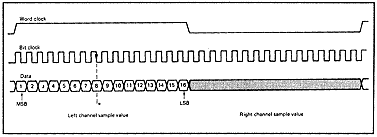
Shown in Fig. 18 are the three signals available within the F1, which are necessary to transfer data between two units. The F1 is designed around a single converter running at twice the sampling frequency; therefore, left and right samples are alternated at the word clock transitions. The word clock is high while the left channel data is being transmitted, and low during the right channel data transmission.
To ensure correct synchronization between the master clock of two F1 systems, the bit clock transition falls at precisely the center of each data bit which is carried MSB (most-significant bit) first. Short cables are recommended for linking two F1 processors.
Figure 18 - Three signals available within the Sony PCM F1 digital audio processor for transferring data between two units.
[Index | Main Paragraph | Next Paragraph ]